Difference between revisions of "Multimodal microscopy"
Montgomery (talk | contribs) |
Montgomery (talk | contribs) |
||
| Line 28: | Line 28: | ||
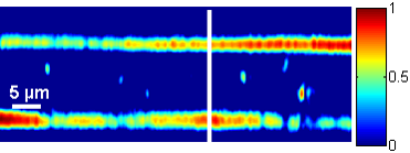
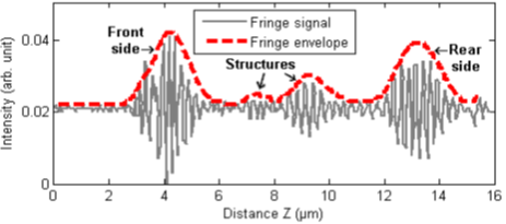
:'''Tomography''': high-resolution characterization of thick (>500 nm) transparent, semi-transparent or translucent layers of materials such as glass layers, polymer films, colloidal layers or layers of hydroxyapatite (biomaterials). Instead of just detecting a single fringe signal corresponding to the surface at each point to measure surface roughness, several fringe signals along the optical axis can be detected at each point that correspond to buried surfaces or structures. To do this, an image stack is built up by scanning the whole depth of the film to be measured followed by image processing to reveal the XZ image, or "B-scan" that shows a cross sectional image of the film and buried structures and is known as OCT (Optical Coherence Tomography). | :'''Tomography''': high-resolution characterization of thick (>500 nm) transparent, semi-transparent or translucent layers of materials such as glass layers, polymer films, colloidal layers or layers of hydroxyapatite (biomaterials). Instead of just detecting a single fringe signal corresponding to the surface at each point to measure surface roughness, several fringe signals along the optical axis can be detected at each point that correspond to buried surfaces or structures. To do this, an image stack is built up by scanning the whole depth of the film to be measured followed by image processing to reveal the XZ image, or "B-scan" that shows a cross sectional image of the film and buried structures and is known as OCT (Optical Coherence Tomography). | ||
| − | <gallery widths= | + | <gallery widths=250px heights=150px> |
File:Mylar tomo défauts.png|High resolution tomographic XZ image of 5 µm thick Milar polymer film with internal defects. | File:Mylar tomo défauts.png|High resolution tomographic XZ image of 5 µm thick Milar polymer film with internal defects. | ||
File:Mylar tomo 2D profile.png|Fringe signal showing top and bottom surfaces and presence of internal defects in Milar polymer film. | File:Mylar tomo 2D profile.png|Fringe signal showing top and bottom surfaces and presence of internal defects in Milar polymer film. | ||
| Line 42: | Line 42: | ||
:The following results show 3D measurements in real time (18 3D images per second) of a metallic contact on silicon moving sideways at a speed of 200 µm/s (x40 Mirau objective, axial range of 5 µm). | :The following results show 3D measurements in real time (18 3D images per second) of a metallic contact on silicon moving sideways at a speed of 200 µm/s (x40 Mirau objective, axial range of 5 µm). | ||
| − | <gallery widths= | + | <gallery widths=120px heights=120px> |
File:Basler_fringesv2c.gif|Continuous fringe scanning on a metallic contact on silicon moving sideways at a speed of 200 µm/s. | File:Basler_fringesv2c.gif|Continuous fringe scanning on a metallic contact on silicon moving sideways at a speed of 200 µm/s. | ||
| − | |||
| − | |||
File:Basler_MAXv3-2.gif|Real time measurement: reflection image with extended depth of focus. | File:Basler_MAXv3-2.gif|Real time measurement: reflection image with extended depth of focus. | ||
| − | |||
| − | |||
File:BaslerALT3Dv4c.gif|Real time measurement: 3D image measured at a rate of 18 3D images/s. | File:BaslerALT3Dv4c.gif|Real time measurement: 3D image measured at a rate of 18 3D images/s. | ||
| − | |||
</gallery> | </gallery> | ||
| Line 61: | Line 56: | ||
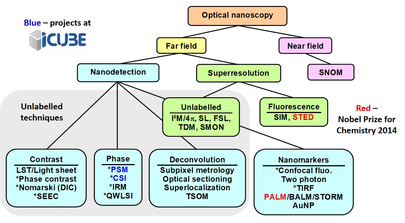
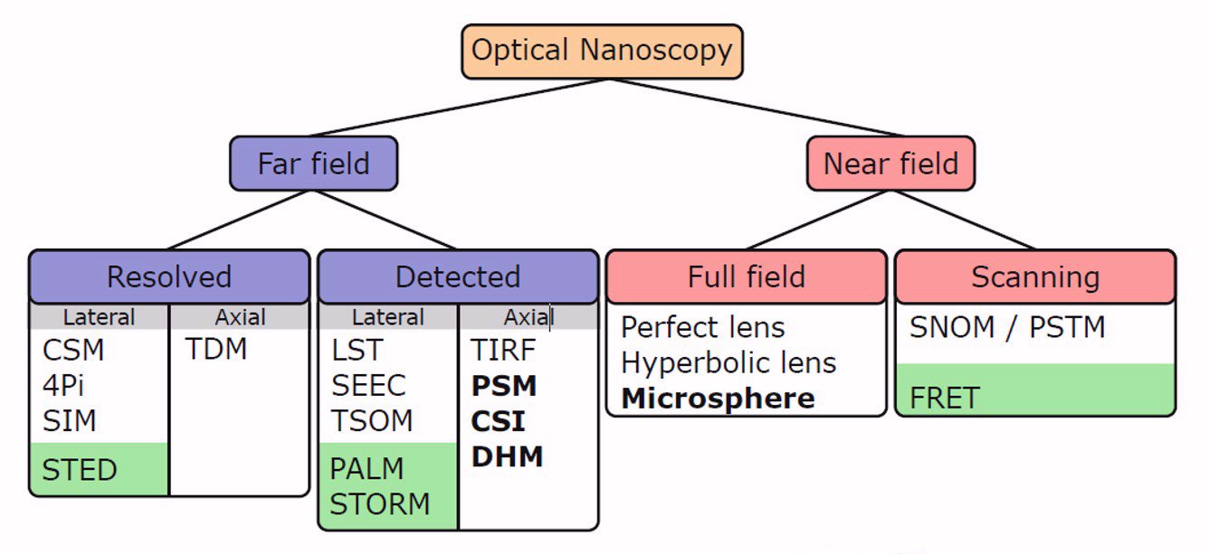
:'''Optical nanoscopy''': study of basic principles of optical nanoscopy techniques for imaging and characterizing microscopic structures with one or more dimensions at the nanometer scale either optically resolved using super-resolution or unresolved but detectable using nanodetection. The two following classification schemes developed give a better perspective of the main techniques available, the second one taking into account microsphere imaging. | :'''Optical nanoscopy''': study of basic principles of optical nanoscopy techniques for imaging and characterizing microscopic structures with one or more dimensions at the nanometer scale either optically resolved using super-resolution or unresolved but detectable using nanodetection. The two following classification schemes developed give a better perspective of the main techniques available, the second one taking into account microsphere imaging. | ||
| − | <gallery widths= | + | <gallery widths=250px heights=250px> |
File:Nanoscopy classification scheme 2017.jpg|A classification scheme for the different nanoscopy techniques (2017). | File:Nanoscopy classification scheme 2017.jpg|A classification scheme for the different nanoscopy techniques (2017). | ||
File:Nanoscopy classification scheme SP SL 2019.jpg|A classification scheme for the different nanoscopy techniques taking into account microsphere imaging (2019). | File:Nanoscopy classification scheme SP SL 2019.jpg|A classification scheme for the different nanoscopy techniques taking into account microsphere imaging (2019). | ||
| Line 71: | Line 66: | ||
:'''Enhanced resolution''': enhanced lateral resolution using glass microspheres to improve the resolving power in 2D reflection microscopy for high detail imaging and in interference microscopy for nanometrology. Studies are performed from both theoretical and experimental points of view. The theoretical study of the imaging properties of microspheres and resolution enhancement is carried out using rigorous 2D FEM simulation under COMSOL. A rigorous model is also being developed for surface topography measurement using interference microscopy and in particular, using Phase Shifting Microscopy (PSM). | :'''Enhanced resolution''': enhanced lateral resolution using glass microspheres to improve the resolving power in 2D reflection microscopy for high detail imaging and in interference microscopy for nanometrology. Studies are performed from both theoretical and experimental points of view. The theoretical study of the imaging properties of microspheres and resolution enhancement is carried out using rigorous 2D FEM simulation under COMSOL. A rigorous model is also being developed for surface topography measurement using interference microscopy and in particular, using Phase Shifting Microscopy (PSM). | ||
| − | <gallery widths= | + | <gallery widths=200px heights=200px> |
File:Contrast function 2D microsphere.png|Improvement in 2D lateral resolution of an optical reflection microscope using microspheres by measuring the contrast transfer function using square gratings. | File:Contrast function 2D microsphere.png|Improvement in 2D lateral resolution of an optical reflection microscope using microspheres by measuring the contrast transfer function using square gratings. | ||
File:Photonic jet lens simulation.png|Simulation using the concept of a photonic jet lens for studying imaging properties of microspheres. | File:Photonic jet lens simulation.png|Simulation using the concept of a photonic jet lens for studying imaging properties of microspheres. | ||
| Line 89: | Line 84: | ||
Results can then be taken from the spectral cube to give the reflectance map at a given wavelength or the reflectance spectra from specific pixels to show the optical properties of different materials. Using colorimetry, the reflectance results can then be used to determine the local colour, or the colour as observed by human eye under typical midday light. This is achieved by first determining the trichromatic components XYZ at each pixel of the spectral cube and then the trichromatic coordinates on the colour locus (CIE 1931 with D65 illuminating spectra). The following results show some experimental measurements compared with the theoretical values of the previous copper layer on glass [https://publis.icube.unistra.fr/2-MCOC23 [S. Marbach et al., Opt. & Las. in Eng., 2023<nowiki>]</nowiki>]: | Results can then be taken from the spectral cube to give the reflectance map at a given wavelength or the reflectance spectra from specific pixels to show the optical properties of different materials. Using colorimetry, the reflectance results can then be used to determine the local colour, or the colour as observed by human eye under typical midday light. This is achieved by first determining the trichromatic components XYZ at each pixel of the spectral cube and then the trichromatic coordinates on the colour locus (CIE 1931 with D65 illuminating spectra). The following results show some experimental measurements compared with the theoretical values of the previous copper layer on glass [https://publis.icube.unistra.fr/2-MCOC23 [S. Marbach et al., Opt. & Las. in Eng., 2023<nowiki>]</nowiki>]: | ||
| − | <gallery widths= | + | <gallery widths=250px heights=250px> |
File:Spectral cube copper glass.jpg|Spectral Cube measured on 2 µm thick layer of copper on glass. | File:Spectral cube copper glass.jpg|Spectral Cube measured on 2 µm thick layer of copper on glass. | ||
File:Spectral map and response copper glass.jpg|Reflectance map at 𝝀 = 720 nm of a copper layer on glass (left) and reflectivity spectra (right) of the copper and the glass. | File:Spectral map and response copper glass.jpg|Reflectance map at 𝝀 = 720 nm of a copper layer on glass (left) and reflectivity spectra (right) of the copper and the glass. | ||
| Line 102: | Line 97: | ||
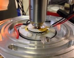
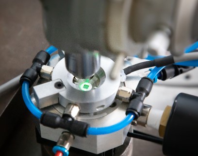
The following example shows the use of environmental chambers under a Linnik microscope to measure the mechanical properties of ultra-thin (30-60 nm) polymer films (collaboration with ICS, Strasbourg). The "nanobubble" inflation method is used, consisting of inflating an array of "nanobubbles" formed by the polymer film on a grid of 5 µm diameter holes. Two prototype chambers were developed, the first to control the temperature and pressure [https://publis.icube.unistra.fr/2-CMAL17 [P. Chapuis et al., Rev. Sci. Instr. 2017<nowiki>]</nowiki>] and the second to control the temperature, pressure and humidity [https://publis.icube.unistra.fr/2-MFAM23 [P. Montgomery et al., ACS Omega, 2023<nowiki>]</nowiki>]. | The following example shows the use of environmental chambers under a Linnik microscope to measure the mechanical properties of ultra-thin (30-60 nm) polymer films (collaboration with ICS, Strasbourg). The "nanobubble" inflation method is used, consisting of inflating an array of "nanobubbles" formed by the polymer film on a grid of 5 µm diameter holes. Two prototype chambers were developed, the first to control the temperature and pressure [https://publis.icube.unistra.fr/2-CMAL17 [P. Chapuis et al., Rev. Sci. Instr. 2017<nowiki>]</nowiki>] and the second to control the temperature, pressure and humidity [https://publis.icube.unistra.fr/2-MFAM23 [P. Montgomery et al., ACS Omega, 2023<nowiki>]</nowiki>]. | ||
| − | <gallery widths= | + | <gallery widths=200px heights=150px> |
File:Nanobubble expt photo.jpg|Leitz Linnik microscope with environmental chamber and control equipment for studying mechanical properties of ultra-thin polymer films. | File:Nanobubble expt photo.jpg|Leitz Linnik microscope with environmental chamber and control equipment for studying mechanical properties of ultra-thin polymer films. | ||
File:Nanobubble chamber 1.jpg|1st prototype of environmental chamber to control temperature and pressure. | File:Nanobubble chamber 1.jpg|1st prototype of environmental chamber to control temperature and pressure. | ||
| Line 110: | Line 105: | ||
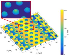
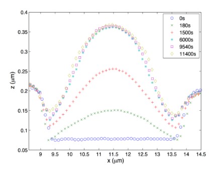
Using the very sensitive technique of PSM, the shape of the "nanobubbles" can be monitored over several hours in order to measure the relaxation and then determine the creep compliance. Measuring at the nanometer scale over such a long period is challenging, requiring the development of a careful measurement protocol in order to obtain significant results. | Using the very sensitive technique of PSM, the shape of the "nanobubbles" can be monitored over several hours in order to measure the relaxation and then determine the creep compliance. Measuring at the nanometer scale over such a long period is challenging, requiring the development of a careful measurement protocol in order to obtain significant results. | ||
| − | <gallery widths= | + | <gallery widths=200px heights=150px> |
File:Nanobubble PSM 3D.jpg|thumb|Measurement using PSM of 3D shape of inflated polymer "nanobubbles" on grid of 5 µm diameter holes. | File:Nanobubble PSM 3D.jpg|thumb|Measurement using PSM of 3D shape of inflated polymer "nanobubbles" on grid of 5 µm diameter holes. | ||
File:Nanobubble relaxaton results.jpg|thumb|Measurement of "nanobubble" relaxation over several hours. | File:Nanobubble relaxaton results.jpg|thumb|Measurement of "nanobubble" relaxation over several hours. | ||
Revision as of 15:27, 7 August 2023
P. Montgomery, M. Flury, F. Anstotz, S. Lecler, V. Maioli, D. Montaner, A. Nahas, F. Salzenstein.
What is multimodal nanoscopy?
The IPP team has been at the forefront of research in the field of interference microscopy for many years. The aims are several. More recently, they concern improving the lateral resolution to beyond the diffraction limit without using markers. The addition of different imaging modalities allows using the same imaging system to access different types of information such as microscopic surface topography (static and moving), the high-resolution structure of transparent layers and the local spectroscopic response. The use of dedicated environmental chambers allows the study of specific parameters of samples in a controlled environment. The study of specific algorithms allows optimisation of fringe processing and the extraction of the required information.
The team is also extending its field of investigation of samples from the historical application areas of materials and micro- nanotechnologies to those of the biological field. It does this through strong links with local actors in the field (ICS, IPCMS, IGBMC, IPHC, etc.), starting from the fundamental understanding of the basic principles involved, through the development of prototype instrumentation, right through to the technology transfer of the techniques developed.
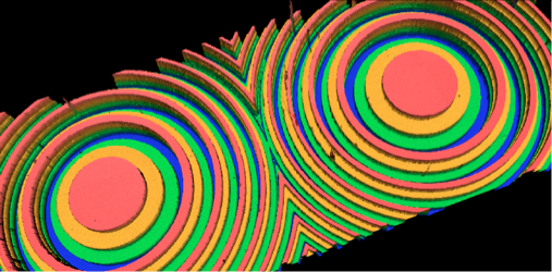
Interference microscopy, often called WLSI (White Light Scanning Interferometry) is typically used to measure nanometric surface roughness using PSM (Phase Shifting Microscopy) and deeper structures using CSI (Coherence Scanning Interferometry).

Deep surface structure: Fresnel microlens measured on the Zygo NewView 7200 white light interferometer.

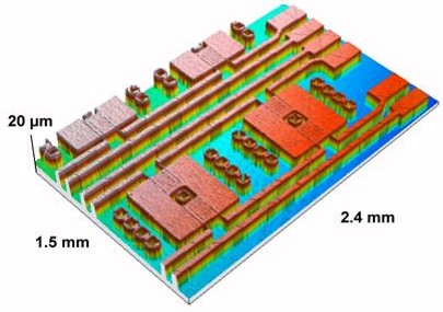
Deep surface structure measured using CSI: CMOS Hall microsensor (SMH, ICube).

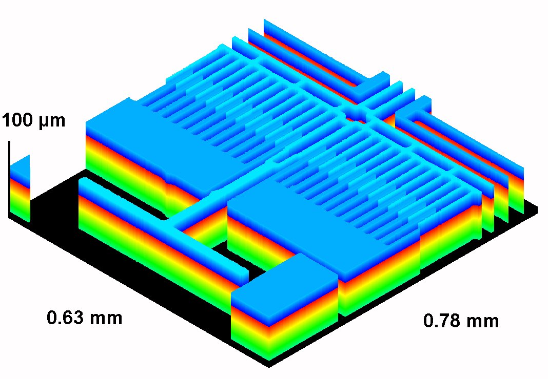
Deep surface structure measured using CSI: MOEMS miniature FT spectrometer (IMT, Neuchâtel, Switzerland).

Nanometric roughness measurement using PSM: laser crystallisation of a-Si for flat screen transistors.
- Scanning interference microscopy is a powerful technique based on far field optical reflection microscopy and interferometry that can be used for extracting information on micro- and nanostructures embedded in complex materials, devices and microsystems. While the technique is classically used for measuring static microscopic surface roughness and topography, we have developed other measurement modes and various techniques for improving the measurements (see review in [P. Montgomery et al., ACS Omega, 2023]).
- The following topics are covered:
- Tomography: high-resolution characterization of thick (>500 nm) transparent, semi-transparent or translucent layers of materials such as glass layers, polymer films, colloidal layers or layers of hydroxyapatite (biomaterials). Instead of just detecting a single fringe signal corresponding to the surface at each point to measure surface roughness, several fringe signals along the optical axis can be detected at each point that correspond to buried surfaces or structures. To do this, an image stack is built up by scanning the whole depth of the film to be measured followed by image processing to reveal the XZ image, or "B-scan" that shows a cross sectional image of the film and buried structures and is known as OCT (Optical Coherence Tomography).

High resolution tomographic XZ image of 5 µm thick Milar polymer film with internal defects.

Fringe signal showing top and bottom surfaces and presence of internal defects in Milar polymer film.
These techniques are also useful for characterising nanostructured photonic devices developed in the theme Photonics Modeling and Simulation.
- 4D microscopy (3D+time): 3D topographic measurement in real time of surfaces that evolve aperiodically, such as moving samples and those found in soft materials, microsystems (MEMS and MOEMS) and chemical reactions. The fringes are scanned continuously over the depth to be measured and a high speed camera is used in combination with fast FPGA (Field Programmable Gate Array) cabled logic processing to give real time measurements of surface roughness and structure.
- The following results show 3D measurements in real time (18 3D images per second) of a metallic contact on silicon moving sideways at a speed of 200 µm/s (x40 Mirau objective, axial range of 5 µm).

Continuous fringe scanning on a metallic contact on silicon moving sideways at a speed of 200 µm/s.

Real time measurement: reflection image with extended depth of focus.

Real time measurement: 3D image measured at a rate of 18 3D images/s.
- Fringe processing algorithms: adaptation of fringe processing techniques for specific imaging modalities. In particular, compact and robust Teager-Kaiser energy operators (TKEO) have been developed for tomography and 4D microscopy and Fourier Transform (FT) algorithms for local spectroscopy measurements together with the Frequency Domain Analysis (FDA) algorithm for the combined high-resolution topography measurements.
- Optical nanoscopy: study of basic principles of optical nanoscopy techniques for imaging and characterizing microscopic structures with one or more dimensions at the nanometer scale either optically resolved using super-resolution or unresolved but detectable using nanodetection. The two following classification schemes developed give a better perspective of the main techniques available, the second one taking into account microsphere imaging.

A classification scheme for the different nanoscopy techniques (2017).

A classification scheme for the different nanoscopy techniques taking into account microsphere imaging (2019).
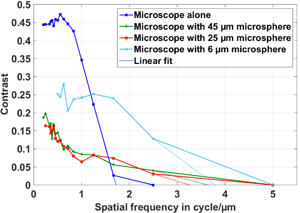
- Enhanced resolution: enhanced lateral resolution using glass microspheres to improve the resolving power in 2D reflection microscopy for high detail imaging and in interference microscopy for nanometrology. Studies are performed from both theoretical and experimental points of view. The theoretical study of the imaging properties of microspheres and resolution enhancement is carried out using rigorous 2D FEM simulation under COMSOL. A rigorous model is also being developed for surface topography measurement using interference microscopy and in particular, using Phase Shifting Microscopy (PSM).

Improvement in 2D lateral resolution of an optical reflection microscope using microspheres by measuring the contrast transfer function using square gratings.

Simulation using the concept of a photonic jet lens for studying imaging properties of microspheres.

Study of the conversion of an evanescent wave into a propagative wave by a 3 µm diameter glass microsphere.

3D measurement of nanoripples on stainless steel using 25 µm glass microsphere in a Linnick interferometer.

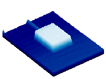
Myelenated nerve fibers from mouse embryo brain using 24 µm diameter glass microsphere in dark field transmission microscopy.
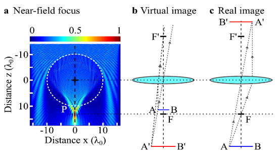
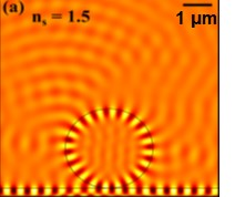
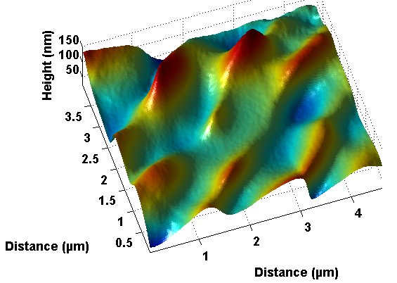
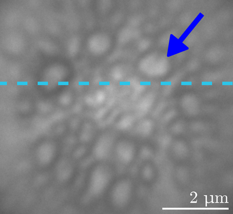
Experimental results of improved resolution imaging and surface topography measurements using microspheres are demonstrated.
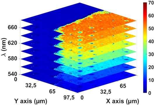
- Local spectroscopy: local characterization of the optical properties of materials, layers and buried interfaces at a local scale of 3.5x3.5 µm and hyperspectral mapping over large areas.
A Linnik interferometer is used to first scan the white light interference patterns along the optical axis to give an interferometric stack. The interferograms at each pixel are then processed using Fourier Transform processing and the modulus of the result gives the "effective spectrum" at each pixel. To remove the optical effects of the instrumentation, the "spectral transfer function" is obtained by measuring a calibrated sample. Dividing the first by the second gives the complete spectral cube containing the spectral reflectivity at each point [S. Marbach et al., Opt. Letts., 2021].
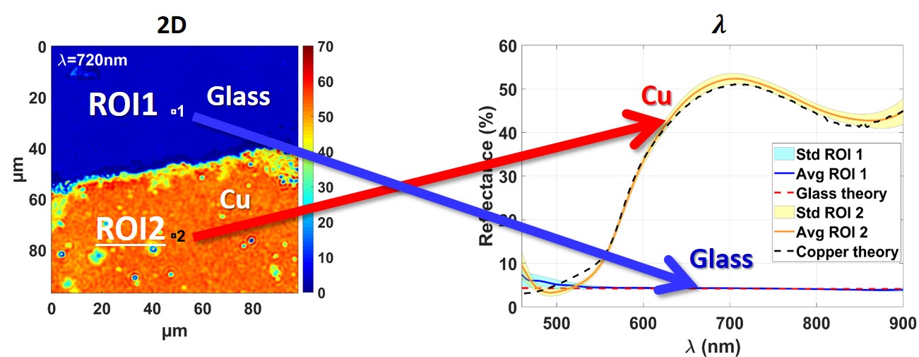
Results can then be taken from the spectral cube to give the reflectance map at a given wavelength or the reflectance spectra from specific pixels to show the optical properties of different materials. Using colorimetry, the reflectance results can then be used to determine the local colour, or the colour as observed by human eye under typical midday light. This is achieved by first determining the trichromatic components XYZ at each pixel of the spectral cube and then the trichromatic coordinates on the colour locus (CIE 1931 with D65 illuminating spectra). The following results show some experimental measurements compared with the theoretical values of the previous copper layer on glass [S. Marbach et al., Opt. & Las. in Eng., 2023]:

Spectral Cube measured on 2 µm thick layer of copper on glass.

Reflectance map at 𝝀 = 720 nm of a copper layer on glass (left) and reflectivity spectra (right) of the copper and the glass.

Experimental (white) and theoretical chromaticity values (black) for glass and copper plotted on colour locus (left) and "real" colour image of the copper layer on glass built from the spectral cube (right).
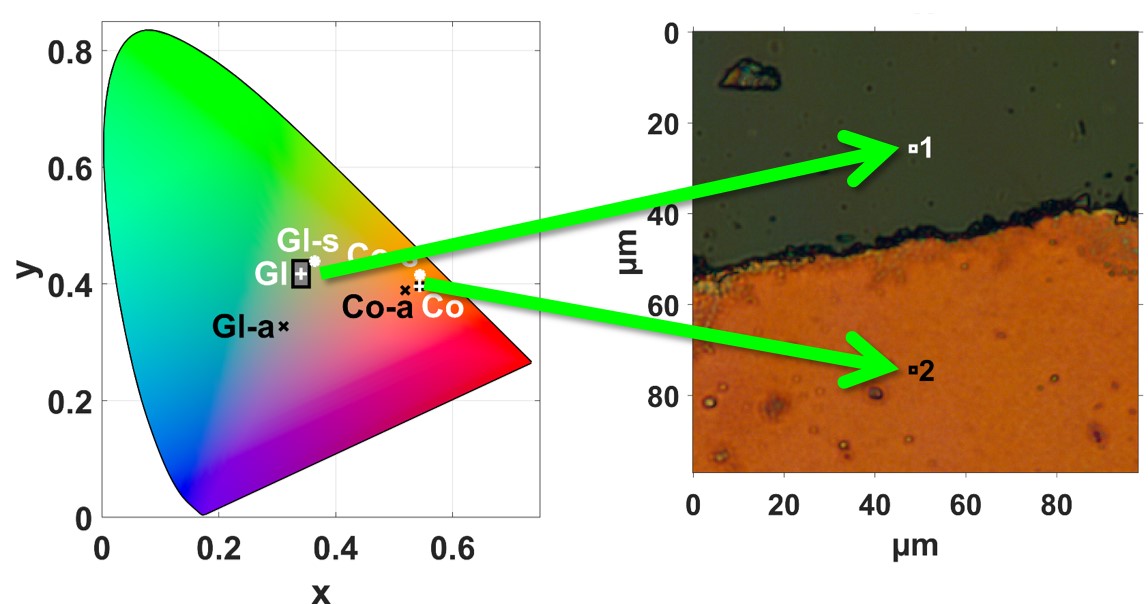
While the colour for copper has been correctly determined, the glass has a slightly yellowish tinge due to the limited illumination spectral range in the blue-UV (460-780 nm).
- Environmental chambers: measurement of specific material parameters using dedicated environmental chambers to control parameters such as temperature, pressure, humidity or the immersion medium.
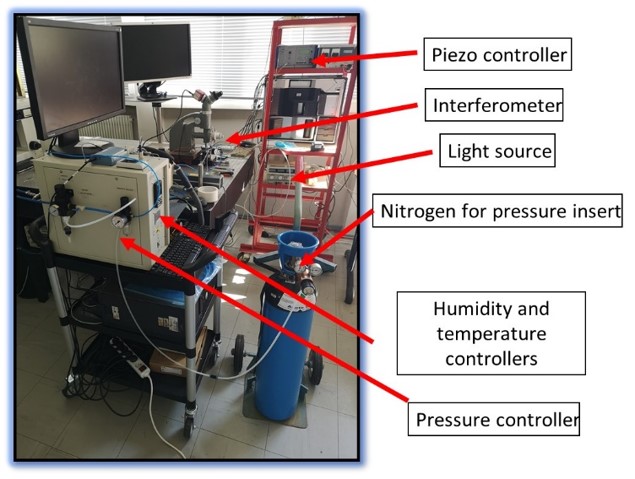
The following example shows the use of environmental chambers under a Linnik microscope to measure the mechanical properties of ultra-thin (30-60 nm) polymer films (collaboration with ICS, Strasbourg). The "nanobubble" inflation method is used, consisting of inflating an array of "nanobubbles" formed by the polymer film on a grid of 5 µm diameter holes. Two prototype chambers were developed, the first to control the temperature and pressure [P. Chapuis et al., Rev. Sci. Instr. 2017] and the second to control the temperature, pressure and humidity [P. Montgomery et al., ACS Omega, 2023].

Leitz Linnik microscope with environmental chamber and control equipment for studying mechanical properties of ultra-thin polymer films.

1st prototype of environmental chamber to control temperature and pressure.

2nd prototype of environmental chamber to control temperature, pressure and humidity.
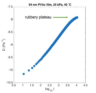
Using the very sensitive technique of PSM, the shape of the "nanobubbles" can be monitored over several hours in order to measure the relaxation and then determine the creep compliance. Measuring at the nanometer scale over such a long period is challenging, requiring the development of a careful measurement protocol in order to obtain significant results.

Measurement using PSM of 3D shape of inflated polymer "nanobubbles" on grid of 5 µm diameter holes.

Measurement of "nanobubble" relaxation over several hours.

Determination of dynamic creep compliance of polymer film (PVAc).
- Other types of microscopy are also being developed, particularly for biomedical applications:
- Full field OCT
- Light sheet microscopy
Funding:
- PHC: Tassili
- ANR: LatexDry
- CNRS: NewMaps ("Time", collaboration with ICS)
- Grand Est region: MIRAGE (FRCR)
- University of Strasbourg: Idex conferences
- SPIE: SPIE Photonics Europe
- ICube internal projects: LocalSpec-PV
Past:
- Indonesian government: 2 Scholarships
- EU INTERREG III
- CNRS: PICS, Cooperation, ACO (collaboration with ESPCI, Paris), pRECISION ("Instrumentation at its limits challenge", collaboration with ICS)
- Grand Est Region: SuperMic (post-doc), MIRAGE (FRCR)
- SATT Conectus Alsace: CAM4D, Nano3D, SIBIC
- Industrial: Eotech SA, Michelin
- ICube internal projects: RTPPP, PiMeNtS, GLOBAL-INNOV