4D Microscopy
4D Microscopy
- The aim of 4D microscopy is to measure and characterize moving or aperiodically changing microscopic structures (MEMS, nanotechnologies, engraving, chemical etching…) using interference microscopy. Our approach is to continuously scan the interference fringes over the whole of the depth of the surface to be measured, to capture the images with a high speed camera and to perform the image processing using highly parallel cabled logic to measure the height of the surface (see « Principle » page). (see « Principe » page).
The CAM 4D project
- The first 4D prototype system was financed by the ACO-CNRS project ("La microscopie optique 3D en temps réel à très haute résolution spatiale") and EU INTERREG III project, in which we succeeded in making measurements in real time at a rate of 6 3D images per second over a depth of several µm [A. Dubois et al., European Phys. J.: Appl. Phys., 2002]. The high speed camera developed in the laboratory allowed an acquisition rate of 250 images/s (512x512 pixels) and the processing was performed using an FPGA ("Field Programmable Gate Array") board.
- Thanks to the CAM4D project financed by Oséo, we were then able to develop a second prototype based on a high speed CMOS camera (500 i/s full field, 16000 i/s with reduced field) with improved real time performance, up to 25 3D images per second over a depth of several µm.
The measurement system
- The prototype consists of two parts. The first one is the Leica DMRX optical microscope equipped with interference objectives (Michelson or Mirau), a light source, a high speed camera, and a piezoelectric vertical translation stage with a range of 100 µm. The latter element is used to scan the fringes over the depth of the sample, the fringes appearing on the camera image of the sample surface. The second part consists of the acquisition board (equipped with a Virtex 2P FPGA Xilinx processor and SRAM or DDR memory) and the PC which controls the translation systems, the image acquisition and storage and the data processing. The whole system has to be carefully synchronised in order for it to function correctly.
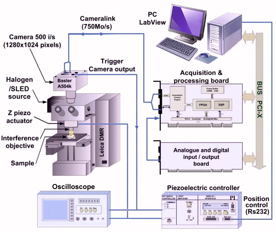
Layout of 4D microscopy system in the CAM4D project.
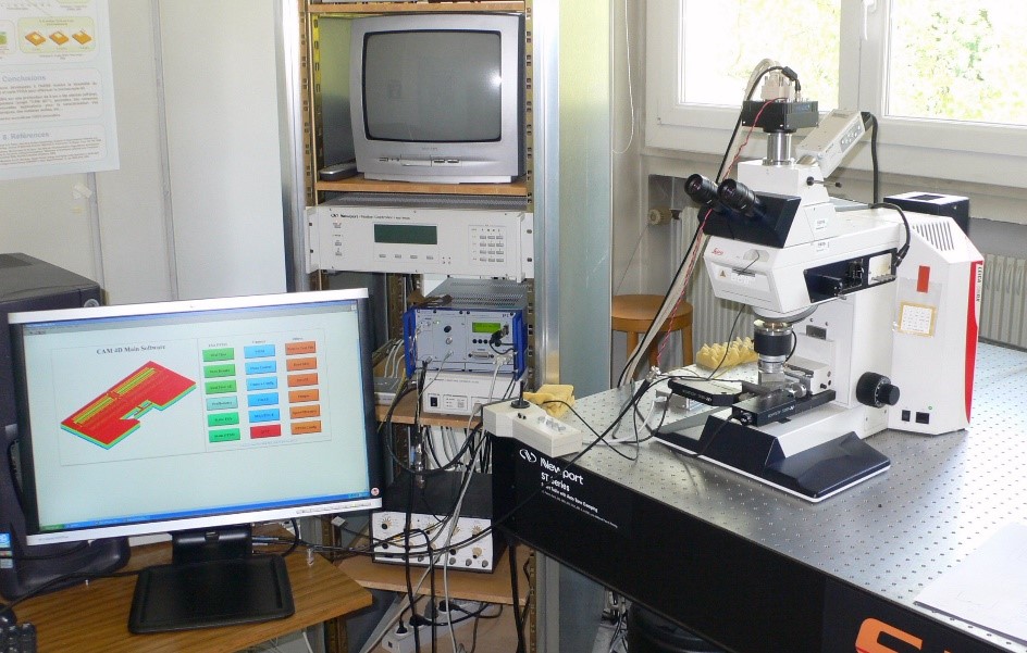
The 4D microscopy system.
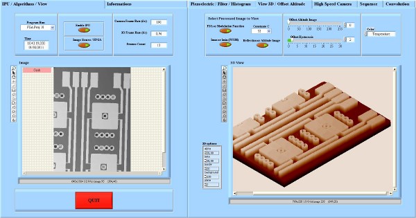
The visualisation software for viewing the results of the CAM 4D system.
- The microscope is placed on a vibration isolation table (SmartTable from NewPort) equipped with a dynamic compensation system to reduce residual vibrations. The scanned fringe images are sent via a « CameraLink » cable to the acquisition board to be processed by the FPGA, where the information about the height at each pixel is extracted. The results are then sent to the PC, where they are visulaised in 3d and analysed. The system has the advantage of being flexible in terms of the choice of the image size, the acquisition rate, the depth to be measured and the type of algorithm used.
The software for controlling the system, for visualising the results and analysing and storing them were developed in a LabView environment.
The algorithms
- The algorithms chosen were very compact, requiring only basic operators such as comparators, additions, multiplexers and multipliers that could be easily implemented in the FPGA. Two algorithms for extracting the surface height in real time were developed in VHDL (Very High speed integrated circuit hardware Description Language) and implemented in the FPGA: PFSM (Peak Fringe Scanning Microscopy) and FSA (Five-Sample-Adaptive non linear algorithm).
PFSM
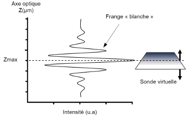
- The PFSM algorithm is very simple, consisting of detecting the peak intensity of the fringe signal, corresponding to the zero order fringe. This fringe peak is used as a virtual probe plane by detecting the highest intensity value at each pixel along the optical axis to measure the positon of the surface at each point and thus the 3D shape. The smaller the sampling step, the higher is the axial resolution but at the cost of more data to process.

Virtual probe plane formed by detection of the peak of the central interference fringe at each pixel in PFSM.
- The PFSM algorithm is well adapted to real time processing on the FPGA since it is fast enough to be applied during the image acquisition. It also has the advantage of being able to vary the axial resolution, typically from 10 nm to 100 nm. The disadvantage of the simplicity is the lack of robustness to variations in background intensity over the scan depth which should not present values higher than the fringe to be detected.
FSA
- The FSA (five Sample Adapative) algorithm consists of detecting the envelope of the fringes by measuring the fringe visibility at each point along the optical axis with a sliding window of 5 consecutive images with phase steps of 90° (λ/8) between images, corresponding to steps of about 76 nm at an average effective wavelength of λ = 610 nm. The following formula is used to calculate the fringe visibility or modulation:

Formula used to calculate the fringe visibility or modulation in FSA, where C is a normalisation constant.

Calculation of the fringe visibility of the signal along the optical axis in FSA.

Detection of the peak of the envelope, giving the position of the surface at that point.
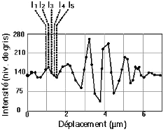
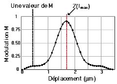
This formula provides a simple means of extracting the envelope of the interference fringes along the optical axis, the peak of which gives the position of the surface at a given pixel. The FSA algorithm is more robust than the PFSM algorithm, being less sensitive to variations in background intensity along the optical axis. While the FSA algorithm has a fixed sampling step of λ/8 between images, the axial resolution can be improved to about 10 nm by interpolation, using for example the least squares method.
Results and performance
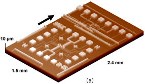
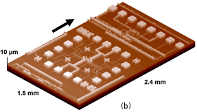
- The following results show the real time "on-line" measurement over a large field size (640 x 1024 pixels) with the PFSM algorithm of a magnetic "microfluxgate" microchip (integrated magnetic probe) being translated laterally at a speed of 20 µm per second by a precision motorised stage. The measurement rate was 1.9 3D images per second over a depth of 5 µm and with an axial resolution of 40 nm.

Real time measurement of a magnetic probe chip moving sideways at a speed 20 µm/s (I0 : t = 0 s; dx = 0 µm).

The eighth 3D image after translation over 84.6 µm (I8 : t = 4,21 s; dx = 84.6 µm).

The height image in PFSM containing the measurement data.

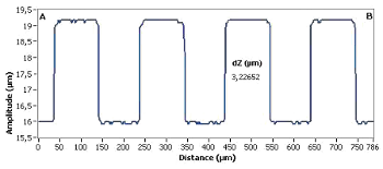
A corresponding 2D profile of part of the sample, showing a depth of 3.22 µm.

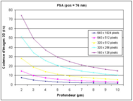
- Real time measurements made on the laboratory prototype have validated the use of the PFSM and FSA algorithms and the theoretical performance. The graphical results below for the two algorithms give the measurement rate as a function of depth for different image sizes. For example, for an image size of 640 x 1024 pixels, a rate of several 3D images/s can be achieved. Reducing the image size to 320 x 256 pixels allows this rate to be increased to around twenty 3D images/s. while the resolution of the FSA algorithm is fixed at around 76 nm, that of the PFSM algorithm can be varied. Increasing the step size increases the measurement rate proportionally (but for a lower axial resolution) whereas decreasing the step size decreases the measurement rate (but for a better axial resolution).

The theoretical 3D on-line measurement rates of the PFSM algorithm for real time measurement as a function of the depth and the image size (for a step = 40 nm).

The theoretical 3D on-line measurement rates of the FSA algorithm for real time measurement as a function of the depth and the image size (for a step size = 76 nm).

Summary of the CAM 4D system
- The 4D microscopy system developed in the CAM 4D project based on a high speed CMOS camera and FPGA processing allows surface roughness and shape to be measured in real time, enabling moving or changing samples to be measured. The technique has the advantages of flexibility in terms of the choice of image size, 3D measurement rate, depth of measurement and algorithm used (PFSM or FSA). The technique opens up new measurement applications.