Difference between revisions of "Photonic jet"
(Created page with "fr:Jet photonique What is it?") |
|||
| (9 intermediate revisions by 2 users not shown) | |||
| Line 1: | Line 1: | ||
[[fr:Jet photonique]] | [[fr:Jet photonique]] | ||
| − | What is | + | Our team has been studying the physics and applications of photonic jets since 2004. We have received for this work the '''first price of the Photonics Innovation Village''' at Photonics Europe (Brussels) in 2016. |
| + | |||
| + | '''What is a photonic jet?''' | ||
| + | |||
| + | When light interacts with a dielectric microsphere, the light is scattered in the far field. However in the near field, the same light can be highly concentrated. In the optimum case, the radiated power density can be concentrated more than 200 times in a propagative beam, having a low divergence and a full width at half-maximum that is smaller than the wavelength. This beam is known as a "photonic jet". Its physical laws are different to those of classical geometrical optics. We have recently demonstrated that they can also be obtained using optical fiber tips. | ||
| + | |||
| + | <gallery widths=200px heights=150px> | ||
| + | File:Jet R24 N15.jpg|Photonic Jet - E field - silica sphere of 24 µm - wavelength 1 µm | ||
| + | File:YAG_jetphot.jpg|Etching setup for beads illumination using a NIR nanoseond laser | ||
| + | File:Jet photonique en embout de fibre.png|Photonic jet achieved using an optical fiber tip. | ||
| + | </gallery> | ||
| + | |||
| + | '''Our work deals with:''' | ||
| + | *Modeling and understanding of the physical phenomenon. | ||
| + | *Laser micro-etching by photonic jet using an ns NIR laser (collaboration with IREPA Laser). | ||
| + | *Enhancement of non-linear fluorescence by photonic jet (collaboration with IPCMS). | ||
| + | *Study of the phenomon in the radiofrequency domain (collaboration with the Hubert Curien Lab at Saint-Etienne). | ||
| + | |||
| + | '''We have recently demonstrated:''' | ||
| + | *That silicon and metals can be etched at 1 µm scale using a photonic jet with a classical nanosecond Nd-YAG laser(40 times smaller than without the photonic jet). | ||
| + | *That with the same laser, despite its low absorption, glass can also be etched (whereas usually a picosencond laser is required). | ||
| + | *That photonic jets can also be obtained at the end of a planar waveguides in the radiofrequency domain and using optical fiber tips in the visible range. | ||
| + | {{#widget:YouTube|id=wjlWnpZlv_w}} | ||
| + | |||
| + | '''Funding:''' | ||
| + | *LaserJet Project (SATT Conectus Alsace). A patent has been applied. | ||
| + | *Jetphot Project (Telecom Institut) | ||
| + | *Jetphot+ Project (Mines-Telecom Institut, IREPA Laser) | ||
| + | *Scholarship of the Indonesian government | ||
| + | |||
| + | <gallery widths=200px heights=150px> | ||
| + | File:Flyer Photonic Jet Station V3.pdf|Photonic jet etching process demonstrator | ||
| + | </gallery> | ||
| + | |||
| + | Download the flyer describing our photonic jet etching process demonstrator that received the first price of the Photonics Innovation Village at Photonics Europe (Brussels) in 2016: [[Média:Flyer Photonic Jet Station V3.pdf]] | ||
Latest revision as of 15:18, 6 June 2016
Our team has been studying the physics and applications of photonic jets since 2004. We have received for this work the first price of the Photonics Innovation Village at Photonics Europe (Brussels) in 2016.
What is a photonic jet?
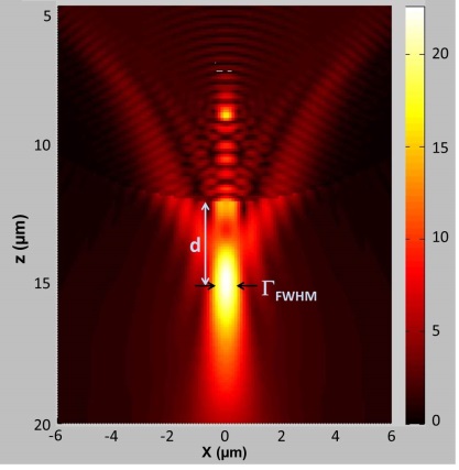
When light interacts with a dielectric microsphere, the light is scattered in the far field. However in the near field, the same light can be highly concentrated. In the optimum case, the radiated power density can be concentrated more than 200 times in a propagative beam, having a low divergence and a full width at half-maximum that is smaller than the wavelength. This beam is known as a "photonic jet". Its physical laws are different to those of classical geometrical optics. We have recently demonstrated that they can also be obtained using optical fiber tips.

Photonic Jet - E field - silica sphere of 24 µm - wavelength 1 µm

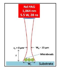
Etching setup for beads illumination using a NIR nanoseond laser

Photonic jet achieved using an optical fiber tip.
Our work deals with:
- Modeling and understanding of the physical phenomenon.
- Laser micro-etching by photonic jet using an ns NIR laser (collaboration with IREPA Laser).
- Enhancement of non-linear fluorescence by photonic jet (collaboration with IPCMS).
- Study of the phenomon in the radiofrequency domain (collaboration with the Hubert Curien Lab at Saint-Etienne).
We have recently demonstrated:
- That silicon and metals can be etched at 1 µm scale using a photonic jet with a classical nanosecond Nd-YAG laser(40 times smaller than without the photonic jet).
- That with the same laser, despite its low absorption, glass can also be etched (whereas usually a picosencond laser is required).
- That photonic jets can also be obtained at the end of a planar waveguides in the radiofrequency domain and using optical fiber tips in the visible range.
{{#widget:YouTube|id=wjlWnpZlv_w}}
Funding:
- LaserJet Project (SATT Conectus Alsace). A patent has been applied.
- Jetphot Project (Telecom Institut)
- Jetphot+ Project (Mines-Telecom Institut, IREPA Laser)
- Scholarship of the Indonesian government

Photonic jet etching process demonstrator
Download the flyer describing our photonic jet etching process demonstrator that received the first price of the Photonics Innovation Village at Photonics Europe (Brussels) in 2016: Média:Flyer Photonic Jet Station V3.pdf